High Reliability, Cost Effective,
5 Days Ship Out
-
PRODUCT
-
Coaxial Cable Assembly
-
Multi-coaxial Cable Assembly
-
Semi-Rigid Cable Assembly
-
LMR Series Cable Assemblies
-
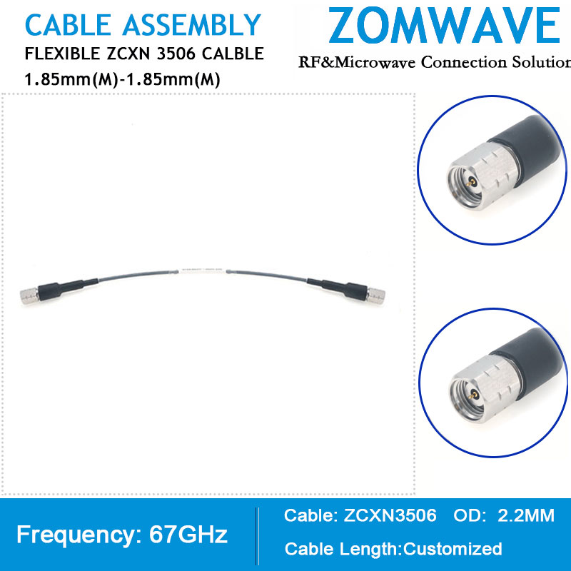
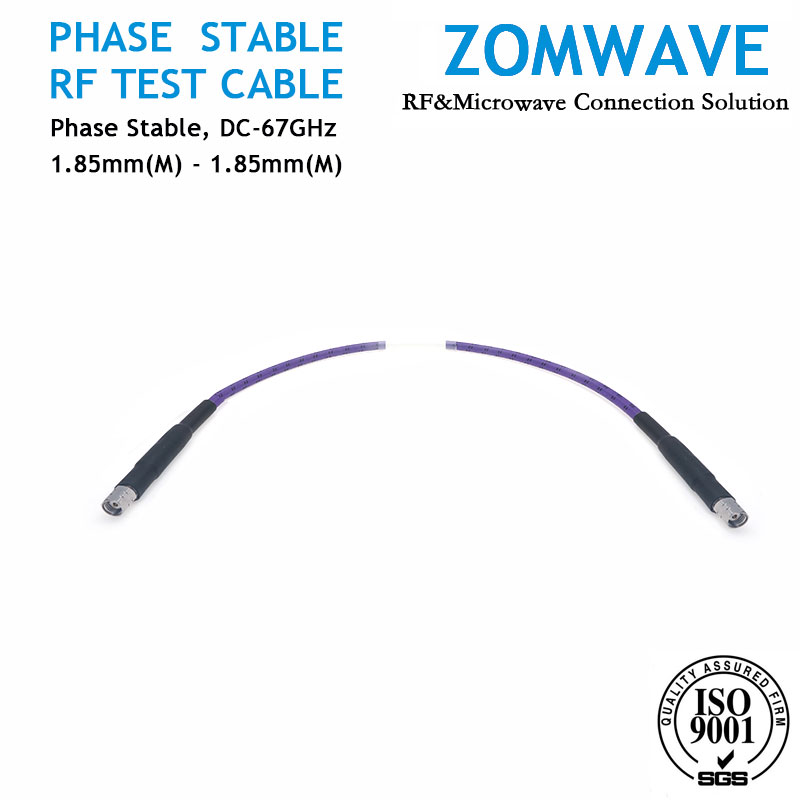
1.85mm to 1.85mm Cable Assembly
-
1.85mm to 2.4mm Cable Assembly
-
1.85mm to 2.92mm Cable Assembly
-
1.85mm to Mini SMP (SMPM/GPPO) Cable
-
2.4mm to 2.4mm Cable Assembly
-
2.4mm to 2.92mm Cable Assembly
-
2.4mm to Mini SMP (SMPM/GPPO) Cable
-
2.92mm to 2.92mm Cable Assembly
-
2.92mm to Mini SMP (SMPM/GPPO) Cable
-
2.92mm to SMP (GPO) Cable Assembly
-
2.92mm to SMA Cable Assembly
-
3.5mm to 3.5mm Cable Assembly
-
3.5mm to SMP Cable Assembly
-
3.5mm to SMA Cable Assembly
-
SMP to SMA Cable Assembly
-
SMP to Type N_TNC_BNC Cable Assembly
-
Mini SMP to Mini SMP Cable Assembly
-
Mini SMP to SMP Cable Assembly
-
Mini SMP to SMA Cable Assembly
-
SMA to TNC Cable Assembly
-
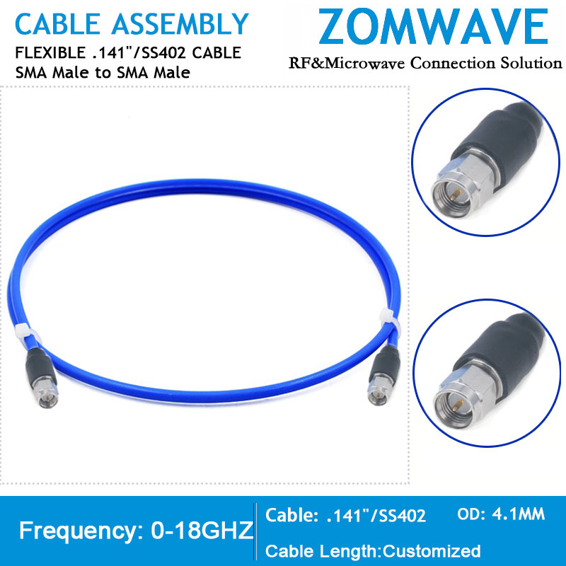
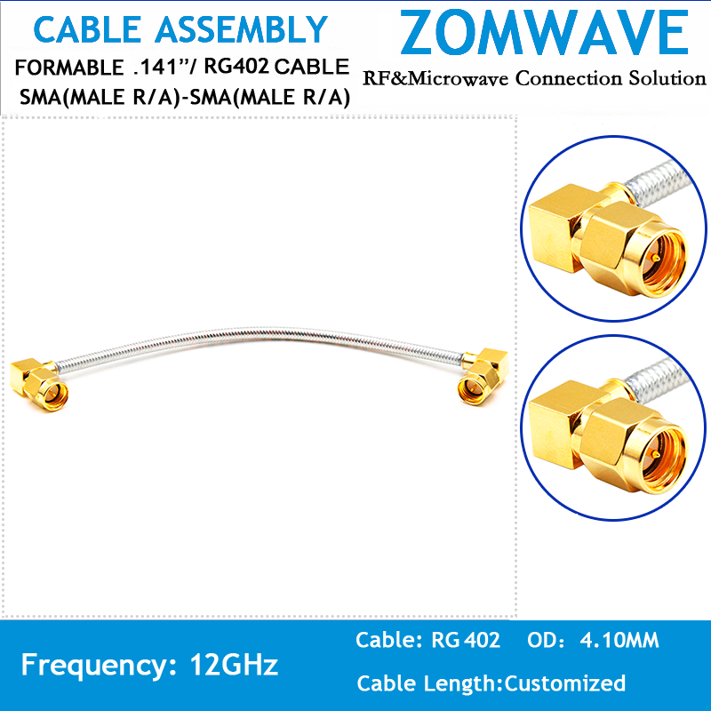
SMA to SMA Cable Assembly
-
SMP to SMP Cable Assembly
-
SMA to SSMA Cable Assembly
-
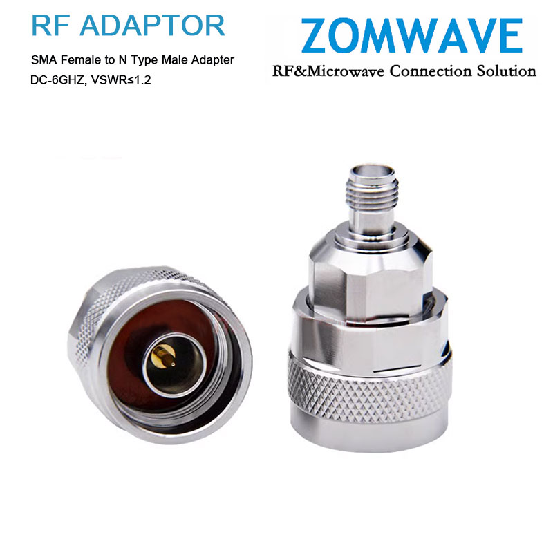
SMA to Type N Cable Assembly
-
SMA to SMB Cable Assembly
-
SMA to MCX Cable Assembly
-
SMA to MMCX Cable Assembly
-
SMA to SSMB Cable Assembly
-
SMA to BNC Cable Assembly
-
Type N Cable Assembly
-
Type N to MCX Cable Assembly
-
Type N to MMCX Cable Assembly
-
Type N to TNC Cable Assembly
-
Type N to BNC Cable Assembly
-
Type N to SMB Cable Assembly
-
TNC Cable Assembly
-
BNC Cable Assembly
-
FAKRA Cable Assembly
-
MCX Cable Assembly
-
MMCX Cable Assembly
-
SMB to SMB Cable Assembly
-
SMB to SMC Cable Assembly
-
SMB to MMCX Cable Assembly
-
SMB to MCX Cable Assembly
-
SMC to SMC Cable Assembly
-
SSMC to SSMC Cable Assembly
-
IPEX(UFL) Cable Assembly
-
IPEX(UFL) To SMA Cable Assembly
-
-
Coaxial RF Connector
-
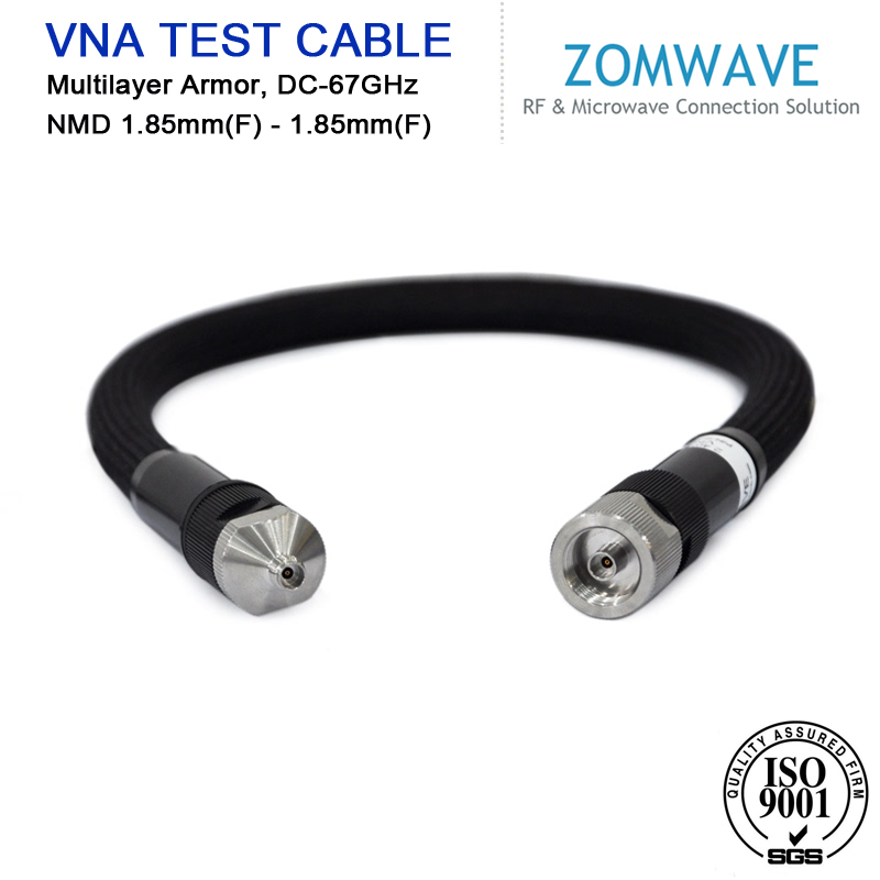
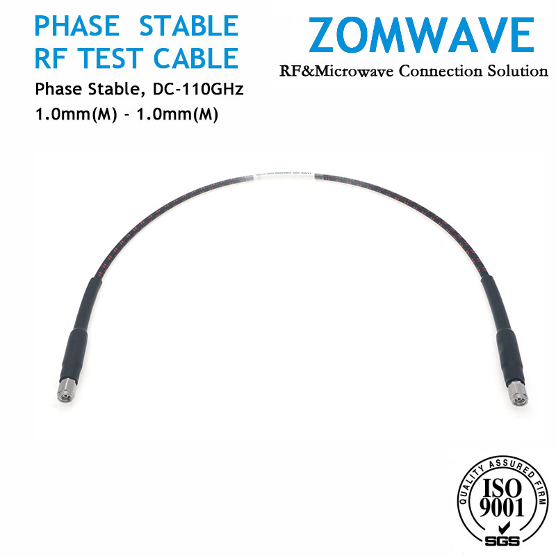
Microwave Test Cable
-
Coaxial RF Adapter
-
1.85mm to 1.85mm Adapter
-
1.85mm to 2.4mm Adapter
-
1.85mm to 2.92mm Adapter
-
2.4mm to 2.4mm Adapter
-
2.4mm to 2.92mm Adapter
-
2.4mm to 3.5mm Adapter
-
2.4mm to Type N Adapter
-
2.92mm to 2.92mm Adapter
-
2.92mm to 3.5mm Adapter
-
2.92mm to SSMA Adapter
-
2.92mm to Type N Adapter
-
3.5mm to 3.5mm Adapter
-
3.5mm to SSMA Adapter
-
3.5mm to BMA Adapter
-
3.5mm to SBMA Adapter
-
3.5mm to Type N Adapter
-
3.5mm to 7mm Adapter
-
SMP to 2.4mm Adapter
-
SMP to 2.92mm Adapter
-
SMP to 3.5mm Adapter
-
SMP to SMA Adapter
-
Mini SMP to 2.4mm Adapter
-
Mini SMP to 2.92mm Adapter
-
Mini SMP to SSMA Adapter
-
Mini SMP to SMA Adapter
-
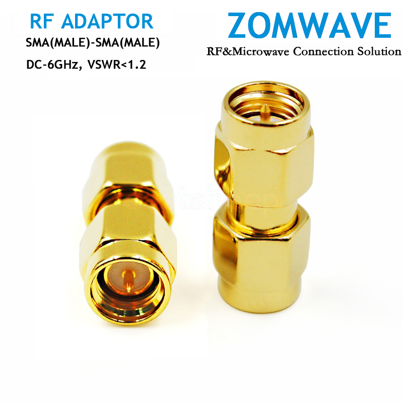
SMA to SMA Adapter
-
SMA to Type N Adapter
-
SMA to SMB Adapter
-
SMA to SMC Adapter
-
SMA to SSMC Adapter
-
SMA to MCX Adapter
-
SMA to MMCX Adapter
-
SMA to IPEX Adapter
-
SMA to BNC Adapter
-
SMA to TNC Adapter
-
SMA to RP-SMA Adapter
-
Type N to Type N Adapter
-
Type N to TNC Adapter
-
Type N to BNC Adapter
-
Type N to RP-SMA Adapter
-
TNC to TNC Adapter
-
TNC to BNC Adapter
-
BNC to BNC Adapter
-
75ohm to 50hom Adapter
-
NMD Adapter
-
-
Coaxial RF Test Probe
-
Coaxial RF Terminator/Load
-